Metallography Capability and Methodology at Electro-Spec Inc.
ESI has multiple analytical tools available to satisfy specific customer requirements along with military and industrial standards. Among these are Cross-Sectioning capabilities, Metallography, Scanning Electron Microscope, (SEM), and Energy Dispersive Spectroscopy, (EDS). These tools are also used in conjunction with plating wisdom to troubleshoot problematic plating deposits on varying materials.
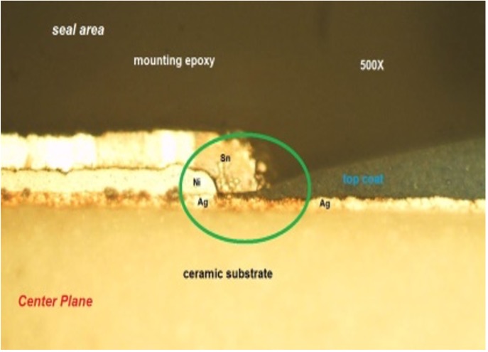
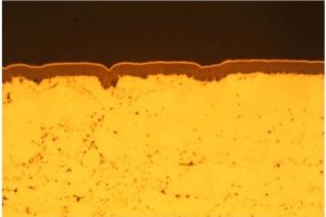
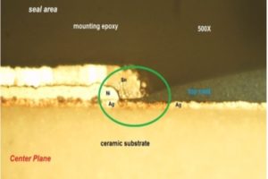
Cross-sectioning, having been in use since the 19th century, is one of the oldest tools in a competent plater’s toolbox. This involves mounting a sample in a material that can then be ground and polished, (i.e. 2-part epoxy mounting material), for further investigation. Standard cross-sectioning techniques provide basic information such as multiple plating layer thicknesses. Beyond standard cross-sectioning techniques, micro cross-sectioning can provide determination of defects in the micro-structure of deposit and substrate for root cause/failure analysis. Parts can also be mounted in conductive epoxy in order to be analyzed with SEM/EDS for a more thorough and detailed plating thickness and elemental analysis.
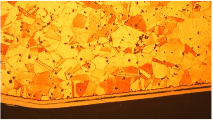
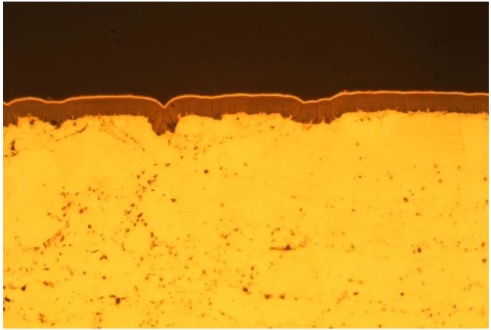
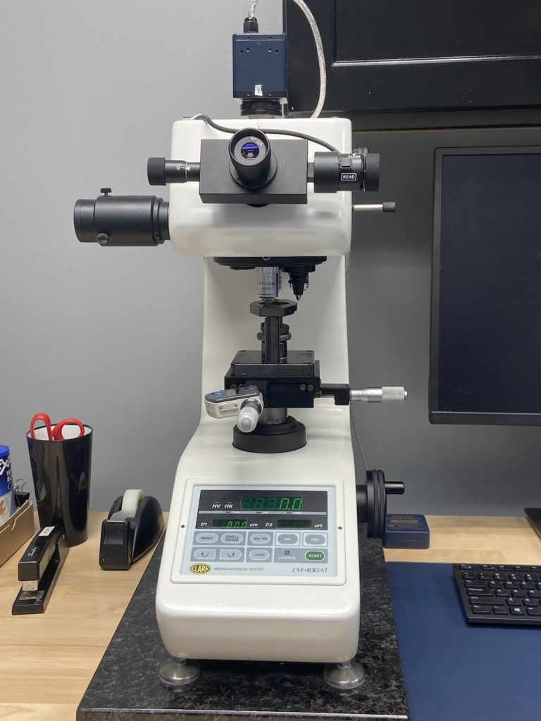
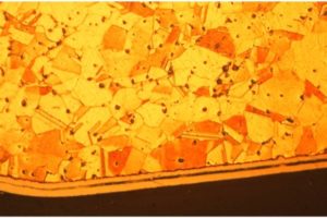
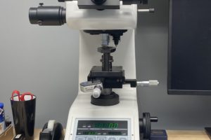
A Metallograph is used for understanding metallurgy at the microstructure level of a given material. It provides an intense bright field in a thin, highly reflective focal plane that is necessary to determine grain structures and grain boundaries of base and plated metals at 50x-1000x. An operator can use different optical filters, prisms, and effects including Differential Interference Contrast, (DIC), which can be used for further defect analysis. For a skilled operator, a Metallograph is a quick and easy tool to use for troubleshooting activities.
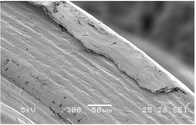
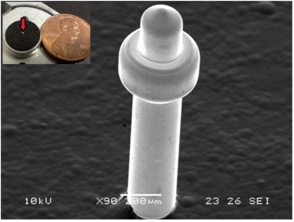
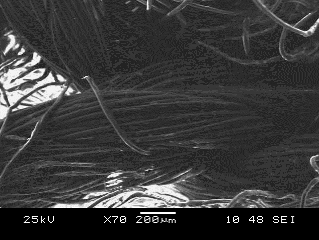
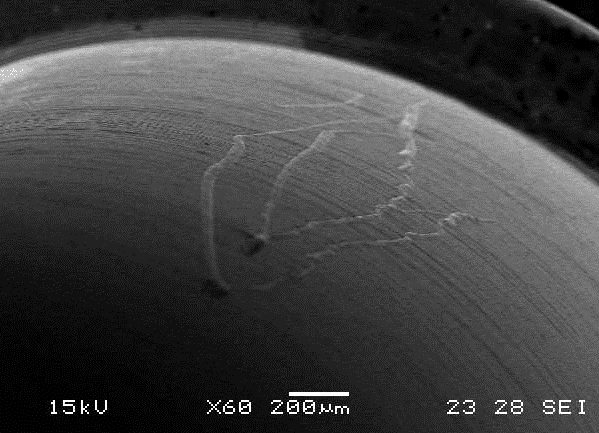
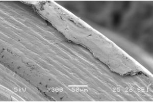
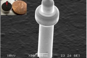
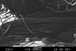
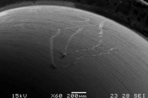
The SEM is a non-optical microscope that uses energized electrons to reflect off of the surface of the sample to create an image. A metallic sample will reflect back good imagery without any prior preparation. Non-metallic items will morph and charge up without any prior preparation. This preparation would include a metal/carbon sputter coater. SEM detection can be made to be extremely sensitive to surface contamination and topography due to the 3D imaging and large magnification factor available. It is exceptionally useful when used in conjunction with X-ray spectroscopy. Cross-sections can be utilized in the SEM/EDS but must use conductive media with the mounting material.
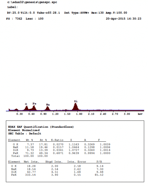
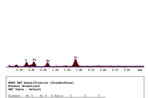
As previously mentioned, SEM/EDS is an X-ray spectroscopy used with an SEM. This provides elemental identification but cannot identify molecular structure except in very rare instances. SEM/EDS is extremely useful for FOD, (Foreign Object Debris), identification and analysis by interrogating individual particles at high magnification, (up to 10,000x). SEM/EDS can also be used for elemental surface mapping. ESI utilizes this ability for FOD contamination/dispersion.
With ESI’s metallurgical tool set, up to and including SEM/EDS, we are able to provide our customer and supplier base with advanced troubleshooting and failure analysis on a variety of parts. ESI has a track record of assistance with defect investigations, root cause analysis, and process optimization.
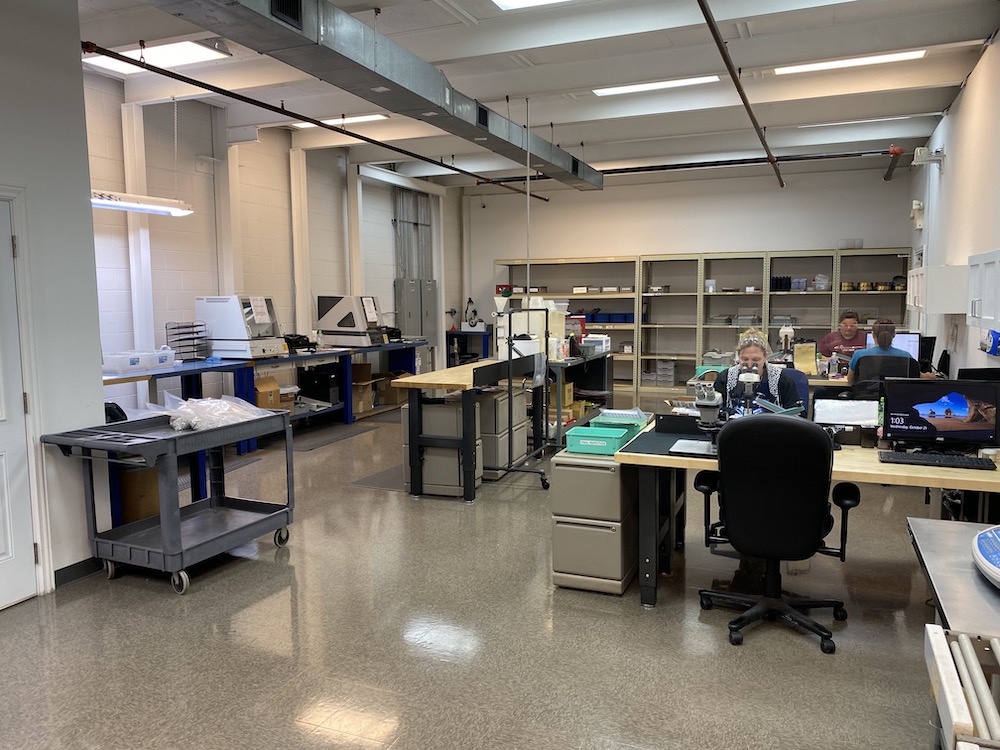
Using a series of steps, ESI has the capability to process defect samples thoroughly beginning with standard stereo-microscope visual inspection, which transitions into cross-sectioning in conjunction with the Metallograph, and if necessary, further cross-sectioning utilizing SEM/EDS. This failure analysis road map provides ESI’s customer and supplier base with various data points and images for enhanced conclusions.
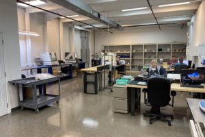
ESI is able to fully exploit this enhanced capability by having a staff of skilled and knowledgeable individuals who perform the analysis. ESI’s staff has the ability to make determinations based on experience that places us at a top level for surface finishing analysis and investigation.


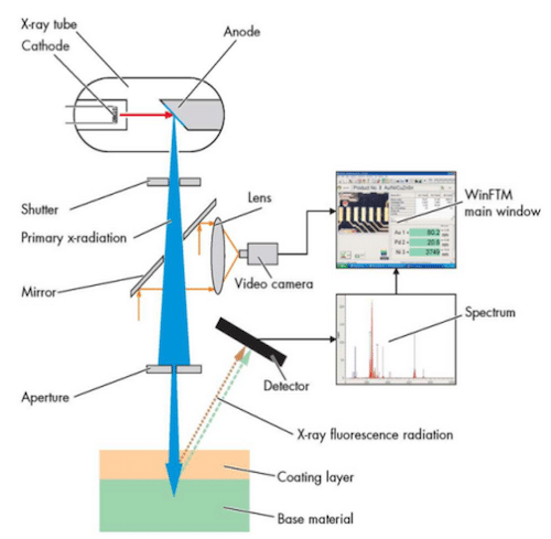 X-Ray Fluorescence (XRF) is a fast, convenient, and non-destructive method used for material analysis, elemental composition, and plating thickness testing for all types of materials. This measurement method is recognized in several industry standards including the B568-98 ASTM standard. XRF requires no use of chemicals and sample preparation is not necessary. XRF provides an accurate thickness measurement in as little as 15 seconds. This happens by measuring the fluorescent (secondary) X-ray emitted from a sample after it has been excited by a primary X-ray source. Since all of the elements present on the sample have special characteristics that are unique, this allows the XRF to be able to identify each element and makes it an excellent source for qualitative and quantitative analysis of material composition and thickness.